ARM Memory Ordering Model
Embedded Systems: ARM Memory Ordering Model
One of the processor operations that has a big impact on execution performance is memory-based operations. The bottleneck is memory latency—there are multiple types of memory: some are fast to access and some are quite slow. The slower ones can negatively affect overall system performance. However, this mix of fast and slow memories is necessary to some extent. Fast memories like SRAM are quite expensive and used internally for caches, whereas slower ones like DRAM are cheaper and can be implemented in large sizes for data storage. This latency-based mix is essential.
Addressing Memory Latency
There are some techniques to address memory latency overhead. One of them is minimizing how frequently certain address ranges are accessed. One way to do this is by merging memory accesses to the same address range, even if they are scattered throughout the program.
Example
R0 <= 0x20000000   ; R0 holds address 0x20000000
R7 <= 0x20010000   ; R7 holds address 0x20010000

; Memory store operations:
STR R1, [R0]        ; Store 1: Store content of R1 into 0x20000000
STR R2, [R0,#0x4]   ; Store 2: Store content of R2 into 0x20000004
STR R3, [R7]        ; Store 3: Store content of R3 into 0x20010000
STR R4, [R0,#0x8]   ; Store 4: Store content of R4 into 0x20000008
From the above:
- Stores 1, 2, and 4 access the range
[0x20000000 - 0x20000008]. - Store 3 accesses a different address:
0x20010000.
Although store 3 is executed before store 4, it breaks the sequence of accessing the contiguous memory range. If executed as-is, the processor might need three separate write access cycles:
- Burst access for stores 1 and 2.
- Separate access for store 3.
- Another separate access for store 4.
This results in three memory write cycles.
Optimizing via Write Buffers
ARM Cortex-M with AHB2 and AXI buses has write buffers to merge and reorder write accesses. The re-ordered execution could be:
store 1   ; STR R1, [R0]
store 2   ; STR R2, [R0,#0x4]
store 4   ; STR R4, [R0,#0x8]
store 3   ; STR R3, [R7]
In this case:
- Stores 1, 2, and 4 are merged into a single burst write.
- Store 3 happens separately.
Now, we have only two memory write cycles instead of three, reducing memory latency.
---
Memory Models
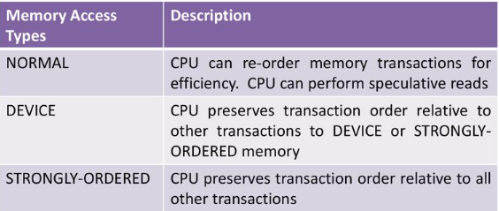
Different memory types allow or disallow transaction ordering and merging. These include:
- Strongly Ordered:
- No reordering allowed
- Access order preserved
- Unaligned access not allowed
- Device:
- No reordering allowed
- Unaligned access not allowed
- Buffered writes to minimize CPU wait time
- Normal:
- Reordering and merging allowed
- Aligned access allowed
- Improves system performance
---
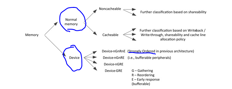
Memory Reconfiguration via MPU
One way to reconfigure the memory model is via the MPU (Memory Protection Unit). You can define memory regions and assign attributes (e.g., cacheable, bufferable) to control memory behavior and performance optimizations.
---
Posted in Embedded Systems | ARM Architecture